Research Report | ASML
Decades of R&D and supply chain mastery make for a deep moat

Note: This version has been updated to present all financial figures in EUR, ASML’s reporting currency. No other changes have been made from the original analysis (previously published in CAD).
I’m excited to share my first research report, diving into ASML Holding N.V. (NASDAQ: ASML). For those who prefer a formatted PDF version, I will be attaching one to this post. All figures are as of March 3, 2025, in EUR.
I’m debating whether to share my valuation model, and may do so in the future, but for now I will be publishing just the write-up. Additionally, I’m considering expanding this into a full deep dive, but I yet to decide whether to devote more time to ASML or move on in search of another interesting company to analyze.

Summary
We recommend a buy on ASML with a target price of €960, a potential upside of 32%, expected within a timeframe of 12 months.
AI boom driving semiconductor demand as hyperscalers invest heavily in next-gen data centers equipped with leading-edge logic & high-performance memory. To meet this demand, chipmakers such as TSMC & Intel are ramping up advanced-node logic production for high-performance computing (HPC) applications, while Samsung & Micron are rapidly expanding DRAM and High Bandwidth Memory (HBM) capacity.
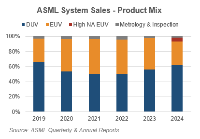
Gross margin expansion driven by EUV becoming a larger share of ASML’s sales mix as foundries ramp 2nm/3nm production and increasing recurring revenue servicing and upgrading existing lithography machines.
ASML’s technological moat strengthens as TSMC & Intel drive early adoption of High-NA EUV, enabling sub-2nm scaling with promising yields and reduced per-wafer costs. Sustained industry-leading R&D investment ensures ASML maintains its monopoly on advanced lithography.
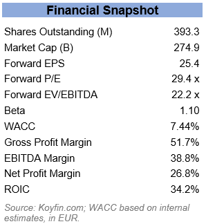
Valuation re-rating potential: ASML trades at ~22x EV/EBITDA, only a 10% premium to peers and close to its 5-year trough, despite outperforming peers on gross margins (51.7%), net margins (26.8%), and ROIC (34.2%). Assigning a conservative 40% premium lifts this multiple to ~29x, aligning with its 5-year average yet well below its historical 110% premium. This leaves ample room for further upside as High-NA ramps and revenue mix improves.
Company Overview
ASML Holding N.V., a Dutch multinational company, is the world leader in manufacturing photolithography equipment for semiconductors. Operating as an integrator, the company outsources most component production. Its technology uses specific light wavelengths to etch precise patterns onto silicon wafers, enabling faster and more efficient computing as these features shrink. The company's key customers are TSMC, Intel, and Samsung. ASML holds exclusive control of extreme ultraviolet (EUV) lithography, which is essential for producing advanced chips used in AI and cloud computing. Their latest innovation, High-NA (Numerical Aperture) EUV lithography, has begun initial shipments to TSMC and Intel for testing and development purposes.
Investment Thesis
ASML is the industry leader in lithography tools, holding a monopoly in EUV and ~80% share in deep ultraviolet (DUV) lithography, reinforced by a complex network of over 5,000 suppliers, €4B in annual R&D, and decades of technical expertise. This R&D and expertise have improved their throughput and yields, reducing per-wafer costs for customers. ASML is positioned to remain the top manufacturer in this space at least the next decade.
EUV is essential for leading-edge chip (<7nm) production, and has been widely adopted by major players such as TSMC, Intel, and Samsung, securing ASML’s role as a critical supplier of wafer fabrication equipment for advanced chips. Now, to manufacture chips below 2nm, ASML has developed next-gen High-NA EUV, and preliminary testing at IMEC, a Dutch research lab and ASML’s R&D partner, shows 20-35% reduction in per-wafer costs compared to previous-gen Low-NA EUV. The first machines have already been delivered to TSMC and Intel, validating the case for High-NA EUV.
Growth Drivers
ASML’s margin expansion and revenue growth will be driven by higher volumes, higher average selling prices (ASP) and a growing share of service and High-NA EUV revenue. Market sentiment is underestimating the durability of ASML’s growth drivers by focusing on near-term volatility. High-NA EUV adoption, driven by structural AI demand, remains a multi-year tailwind.
The AI boom is driving rapid expansion of HPC and HBM production capacity. Training and inference of AI models, such as Large Language Models, requires increasingly powerful and efficient chips, pushing chip producers towards scaling production of leading-edge chips that can only be achieved with ASML’s High-NA EUV tools. TSMC, the leading logic foundry, expects capex to be €39B in 2025, a 33% YoY increase, and is dedicating 70% to scaling advanced node production.
TSMC and Intel’s early acquisition of ASML’s High-NA EUV tools signals its importance for next-gen chip manufacturing. While commercial production isn’t expected until at least 2028, the complexity of lithography requires them to invest in High-NA EUV now to build expertise and improve yields. TSMC’s roadmap includes High-NA EUV high volume manufacturing (HVM) in 2030, but Intel is on track to achieve HVM in 2026. This should pressure TSMC to accelerate its adoption to avoid ceding market share to Intel and maintain its position as the leading foundry. Samsung is targeting 2027 for HVM with High-NA EUV but this timeline will also likely be pulled forward to remain competitive.
Profitability
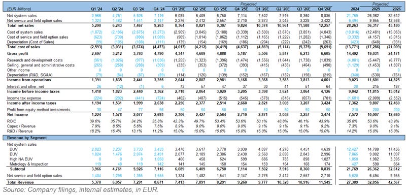
ASML has steadily raised the ASP of EUV and DUV tools at a 10.7% and 4.3% 5Y CAGR, respectively. Greater operating leverage from scale will further enhance profitability, and we project by 2026 ASML will expand annual production capacity to 450 DUV (13% YoY), 50 Low-NA EUV (11% YoY), and 8 High-NA EUV (46% YoY) tools.
Despite a €320M price tag (vs. Low-NA EUV’s €135M), High-NA EUV tools offer stronger unit economics, enabling lower per-wafer costs and increasing customer ROI. A single High-NA EUV exposure can replace 3-4 Low NA EUV passes, driving an estimated payback period of just 2.3 years, vs. 3.1 years for Low-NA EUV. As a result, we estimate High-NA EUV ASP to rise 17% YoY, with Low-NA EUV continuing its 5Y CAGR of 10.7%.
ASML’s service and upgrade business (25% of 2024 revenue) generates significant recurring revenue. As EUV grows in ASML’s revenue mix, we believe this revenue stream will grow 26% YoY and to be margin accretive, as EUV tools generate 150% of their purchase price in service revenue, compared to 130% for DUV.
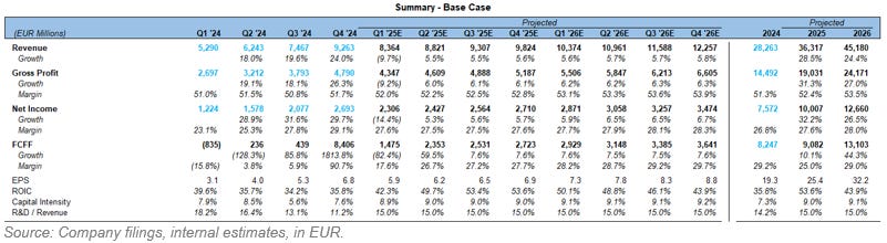
These factors have already lifted ASML’s gross margin from 50.6% to 51.7% (Q1 ’23 - Q4 ’24), and we project gross margin to reach 54.3% by Q4 ’26, with revenue growing at 26.4% CAGR. I’ve modelled R&D at 15% of revenue, the top end of guidance estimates, as ASML will want to invest heavily to reinforce and maintain their technological lead.
Strategic Positioning
ASML recognizes the importance of a reliable supply network and has actively acquired or partnered with key providers. These include Cymer (EUV light source, 2012), Hermes Microvision (inspection equipment, 2016), Berliner Glas Group (optics, 2020), and a 25% stake in Carl Zeiss (optics, 2016). This deep integration makes replication by competitors exceptionally difficult, and they would struggle to match ASML’s margins.
Switching away from ASML’s tools is both risky and costly, as they represent up to 25% of a foundry’s total capex and can remain in use for decades. Local service hubs and regular upgrade cycles further deepen customer lock-in. These factors grant ASML significant pricing power, particularly in High-NA EUV.
ASML aims to distribute a growing dividend, paying out €6.24/share in 2024, a 4.4% increase YoY. This is supplemented with share buybacks, including a current program intended to repurchase ~€12B of shares by the end of 2025.
Risk Factors
In the short term, risks to ASML’s business include foundry capex cuts in the event of a market downturn and further export controls imposed by US and Dutch authorities. While semiconductor end markets are cyclical, the more immediate concern is foundries may delay or reduce capex, impacting tool shipments. In the medium- to long-term, potential competition from alternate technologies exists but remains distant. Canon’s nanoimprint lithography, currently in testing, is limited to 5nm node production, a 2020 technology. Shanghai Micro Electronics Equipment’s EUV patent filing is still early-stage and lacks the throughput or reliability needed for HVM. Commercial disruption from either is unlikely in the next 5 years.
Additionally, as the cost of shrinking transistors rises, manufacturers are exploring architectural innovations like 3D stacking and chiplet design. While these approaches shift some value creation away from lithography steps, they do not displace the need for it. Instead, they often increase overall complexity and wafer demand, reinforcing ASML’s strategic relevance.
Geopolitical risks stem from tensions between Taiwan and China, which claims Taiwan is a part of China’s sovereign territory and has not ruled out use of force to achieve reunification. Roughly 70% of the world’s leading-edge chips are produced in Taiwan, and it is home to TSMC, one of ASML’s largest customers. Conflict in the region could disrupt global semiconductor supply chains and pose a material risk to ASML’s order flow.
Industry & Macro Trends
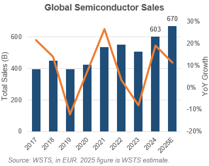
World Semiconductor Trade Statistics (WSTS) reports the global semiconductor industry grew 19% YoY to €602B in 2024, exceeding its €586B forecast, and predicts sales of €671B in 2025, an 11% increase. Leading-edge logic production, ASML’s biggest growth driver, is projected to grow 16%, outpacing total industry capacity growth. As leading-edge nodes become a larger shares of total wafer capacity, EUV adoption is expected to rise proportionally.
ASML is a direct beneficiary of fab expansion cycles, as each new advanced-node foundry requires multiple EUV systems. Global fabrication plant (’fab’) spending was €106B in 2024, up 8% YoY, and projected to rise 4% in 2025 to €154B. Hyperscalers such as Amazon, Google, Microsoft, and Meta are significantly increasing their capex in 2025, committing €306B (+51% YoY) towards new data centers equipped with leading-edge chips. These are expected to come online over the next 2-3 years, creating a sustained revenue tailwind for ASML as foundries ramp up to meet demand.
The US CHIPS Act provides €50B in subsidies to incentivize domestic semiconductor manufacturing, and a 25% investment tax credit applicable to capex on semiconductor manufacturing equipment, including ASML’s lithography tools.
Globally, there has been a push for ‘technological sovereignty’ - for nations to secure domestic manufacturing of chips critical to civilian and military applications. As the sole supplier of EUV tools, ASML stands to benefit from a fragmented but capital-intensive reshaping of the industry.
Valuation
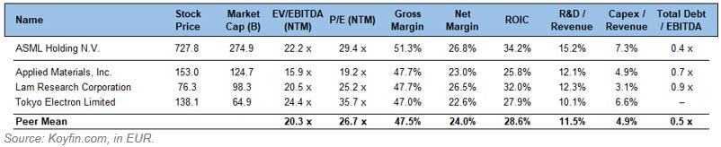
At 22.2x EV/EBITDA, ASML trades roughly in line with its 5-year trough of 22.8x and well below its 43.3x peak and 31.9x average. Relative to peers the stock carries just an 8% premium, vs. its historical average of 110%, despite outperforming peers on gross margins (51.7% vs. 50.5% average), net margins (26.8% vs 25.4% average), and ROIC (34.2% vs 30.9% average) while reinvesting heavily into R&D and maintaining a net-cash balance sheet.
Recent multiple compression was influenced by sharp interest rate hikes alongside broader sector headwinds. As central banks cut rates and semiconductor demand accelerates, fueling foundry capex, re-rating is likely. Applying a conservative 40% premium to the peer average yields a 28.6x EV/EBITDA multiple, consistent with ASML’s historical average and well below prior peaks. This yields a price target of €960, supported by strong revenue growth and margin expansion driven by High-NA EUV adoption. Even under a flat multiple scenario, ASML’s earnings alone would drive significant upside. We forecast no change in ASML’s fundamental positioning, as its market dominance in DUV and monopoly in EUV are intact and unlikely to be credibly challenged in the near- to mid-term.
Peers were selected based on their market cap and dominance in adjacent semiconductor fabrication processes. Applied Materials and Lam Research hold 50% market share in deposition and etch, respectively, and Tokyo Electron has a near-monopoly in coater-developer systems.
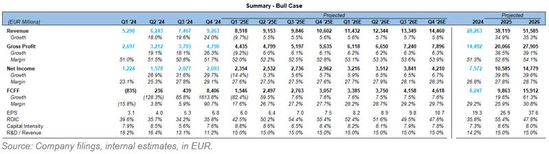
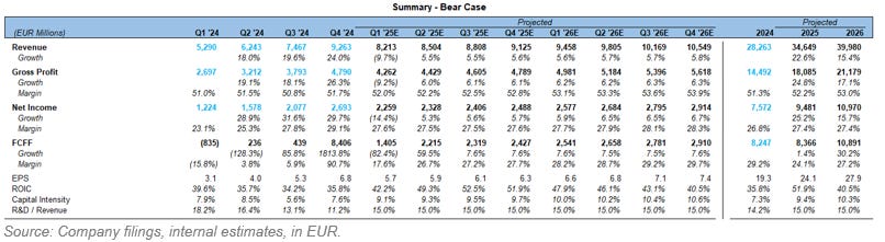
Income Statement & Summary
Disclaimer
At the time of publication, the author holds a long position in ASML.
The information provided in this post is for informational purposes only and does not constitute investment advice, a recommendation, or an offer to buy or sell any securities. Readers should conduct their own research or consult a financial professional before making investment decisions. Investing involves risks, including the potential loss of capital.